Samsung, TSMC Expand Advanced Packaging in Japan
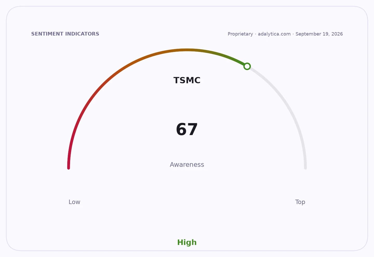
Samsung Electronics and Taiwan Semiconductor Manufacturing Co. are deepening their bets on Japan because the next bottleneck in AI chips is no longer just making smaller transistors — it is how to package and connect them, and Japan controls much of the materials and equipment needed to do it.
Samsung this month fully opened an advanced packaging research base in Yokohama, a project that will cost about 40 billion yen over five years, with Japan’s economy ministry set to subsidize roughly 22.5 billion yen. TSMC, meanwhile, has already opened a 3DIC research center in Tsukuba and is building out its Kumamoto footprint, underscoring how the world’s leading foundry and its closest rival are moving closer to Japanese suppliers and engineers.
The investment wave matters because advanced packaging has become central to AI computing. As leading-edge process shrinks face higher costs and physics limits, chipmakers are leaning on 3D packaging and chiplets to combine GPUs, memory and other dies into a single module. That shift boosts the value of companies such as Ajinomoto, Disco, Tokyo Electron, Resonac and other Japanese materials and equipment makers that sit at the choke points of production.
For investors, the theme points to a broader re-rating of Japan’s semiconductor supply chain. Ajinomoto’s ABF insulating film is widely seen as commanding more than 95% of the market, while Disco is estimated to hold about 80% share in dicing saws and roughly 70% in grinders, and Tokyo Electron is believed to control about 90% of coater-developer systems. Those are the tools and materials that determine yields in advanced packaging, which means Japanese suppliers can capture more value even as chip fabrication itself remains dominated by Taiwan and South Korea.
The geopolitical backdrop is just as important. Taiwan Strait risk, US-China export controls and the push for supply-chain diversification are making Japan look safer as a manufacturing and R&D base. Tokyo has elevated semiconductors to a strategic priority and is using subsidies to pull in foreign capital, while companies are betting that a politically stable, IP-protected ecosystem with dense local supply chains can shorten development cycles.
Market-wise, TSMC’s shares on the NYSE have risen back above their 50-day moving average and closed at $434.67 on Sept. 18, while Samsung Electronics’ Seoul-listed stock ended at 261,000 won, also above its 50-day average. Applied Materials, a key equipment supplier to the sector, closed at $444.57 after a sharp pullback from earlier highs, reflecting the uneven trading in semiconductor capital-equipment names even as the long-term packaging cycle strengthens.
For chipmakers, the strategy is pragmatic: keep the most critical packaging know-how close to the materials and tools they need, spread risk away from Taiwan, and stay competitive in AI supply deals with customers such as Nvidia. For Japan, the risk is that it becomes only a support base unless it keeps its talent, IP and manufacturing know-how anchored at home.
| Entity | Gains | Losses |
|---|---|---|
| Samsung Electronics | ▲Faster AI packaging R&D | ▼Higher Japan capex |
| TSMC | ▲Access to Japanese suppliers | ▼More supply-chain complexity |
| Japanese materials/tools makers | ▲Higher demand, pricing power | ▼Talent poaching risk |
| U.S./Asian chip buyers | ▲Better supply resilience | ▼Higher packaging costs |