Hybrid bonding for high-bandwidth memory is taking longer to reach mass production than the market had expected, a delay that could keep conventional thermal compression bonders in service longer and support Hanmi Semiconductor’s view that its core tool set still has room to run.
Hanmi Semiconductor gains as HBM hybrid bonding slows
That matters because the timing of HBM packaging upgrades is becoming as important as the technology itself. If memory makers and their biggest customer Nvidia do not need to move quickly to hybrid bonding, then capital spending for next-generation bonding equipment is likely to remain focused on established TC tools rather than a premature switch to a more expensive, less mature process.
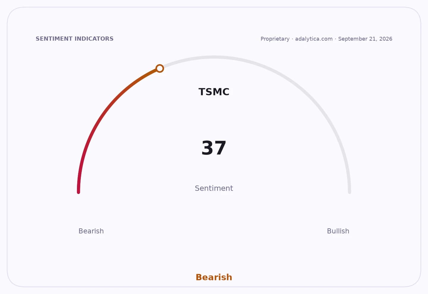
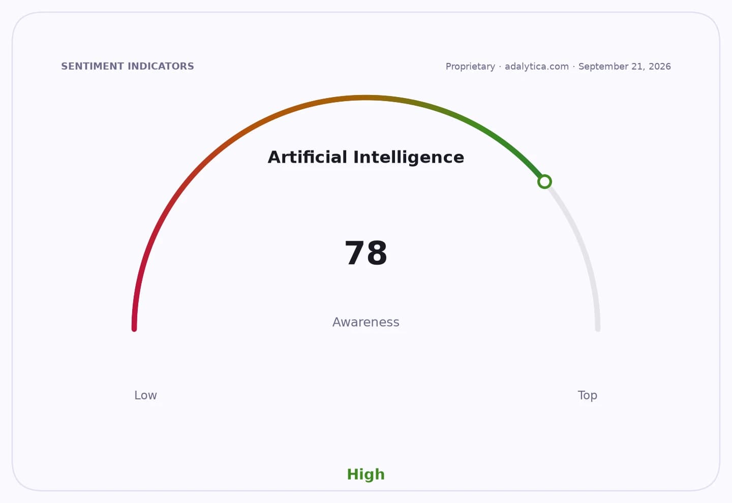
Sentiment IndicatorsⓘProprietary · adalytica.com · September 28, 2026
This is a snapshot — live sentiment, awareness and momentum for 130+ markets update continuously in the dashboard.Open AlphaPulse
At a recent SEMI conference in San Jose, SK Hynix said hybrid bonding would need roughly 90% to 98% yields and a product life of three to five years before it could be put into mass production. The company also pointed to bottlenecks in heat, yield and packaging once HBM is stacked beyond 12 layers, underscoring that the technology is promising but not yet ready for broad deployment.
Nvidia’s own memory road map is reinforcing that caution. The company has been evaluating its next AI accelerator, Rubin Ultra, with a wider set of memory configurations than initially planned, including HBM4E 8-layer and HBM4 8- and 12-layer options, rather than relying only on HBM4E 12-layer parts. That shift reflects uncertainty over validation and manufacturing yields for the highest-density stacks.
For the equipment market, the implication is straightforward: if the industry settles on 8- to 12-layer HBM4 and HBM4E parts for longer, the urgency to migrate to hybrid bonding drops. TC bonders would keep their role in the production line, extending the useful life of the installed base and delaying the revenue inflection some toolmakers had hoped for from a rapid technology transition.
The split in strategy among Korean equipment makers shows how much is riding on that timing call. Hanwha Semitech has positioned hybrid bonding as a potential game changer and has leaned into the idea of an early shift. Hanmi Semiconductor, by contrast, has argued that hybrid bonding will arrive later than many expect, with founder Kwak Dong-shin saying last year that using hybrid bonders for HBM4 and HBM5 would be like using a sledgehammer to crack a nut.
Hanmi has stuck to that view and recently said it plans to broaden the reach of its “wide TC bonder” to HBM5 and HBM6, signaling confidence that TC technology can serve the next few generations of stacked memory. It is also developing hybrid bonders, but only to meet demand when the market is actually ready.
The investment case is therefore less about whether hybrid bonding will matter eventually — it probably will, especially as HBM moves toward 20-layer and higher stacks — and more about when. The longer the industry waits for the yield, reliability and customer demand needed for commercial adoption, the longer TC bonding remains the practical standard.
That leaves Hanmi better placed in the near term, while companies betting on an early hybrid-bonding adoption cycle may have to wait for the market to catch up. For investors, the key catalyst is no longer the promise of the technology itself, but proof that the supply chain can meet the yield thresholds and performance targets needed to justify switching production.
| Entity | Gains | Losses |
|---|---|---|
| Hanmi Semiconductor | ▲Longer TC demand | ▼Early hybrid shift skeptics |
| Hanwha Semitech | ▲None immediately | ▼Early hybrid-bonding bet |
| SK Hynix | ▲More time to prove yields | ▼Faster process migration pressure |
| Nvidia | ▲Flexibility in HBM sourcing | ▼Forced commitment to 12-layer stacks |